Debugging a DOD585-A Analog Delay
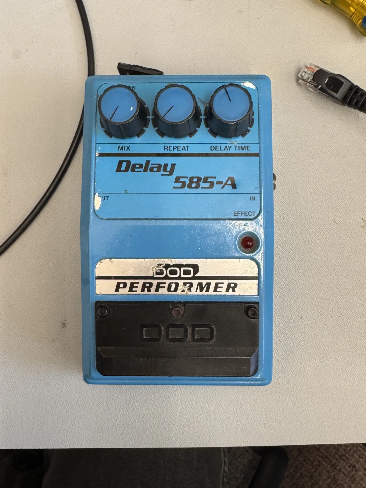
I've had a DOD585 on my bench staring at me for like two months. A local friend asked me to see if I could fix it and I'm always confidently raring to debug stuff right up until the time comes to disassemble and cook at which point I'm always finding reasons not to start. But now I've started and now I'm mostly finished.
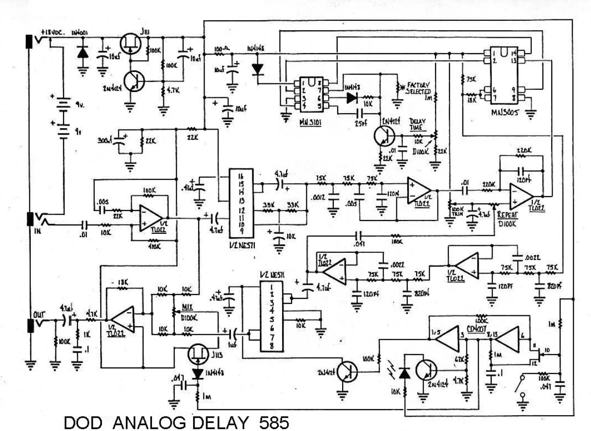
The problem was, when the pedal was on, the signal went to zero when you dialed the mix control all the way up. It only passed clean signal; no delay came out. Fortunately there's a schematic online, so tracing the point of failure was straightforward. Originally, I assumed the problem would be with the MN3005 (the bucket brigade analog delay part) or MN3101 (the clock driver for the bucket brigade part), but everything looked healthy, and I even saw a delayed signal passing all the way to the far side of the AC bypass cap on the output half of the compandor NE5711.
Most of the time hardware debugging is an iterative spiral of guessing what the problem could be, ruling that out, using what you learned from the ruling out process to shorten your list of possible problems, and then firing off another guess and check cycle. Given that delayed signal was making it almost all the way out, and clean signal did make it all the way out, my first guess and check had narrowed the list of possible problems way down. The problem was either with the JFET toggle circuit, or what the JFET toggle circuit was controlling.
If you're not a pedal dork: when we talk about whether or not a pedal is "true bypass" we mean that a non-true bypass pedal routes its signal through a semiconductor controlled buffer path on the PCB instead of through a physical clicky switch (or, more recently, through a microcontroller managed relay). Put another way, a non true bypass pedal is always processing your signal in some small way, even when it's "off."
Boss does this on almost all of their pedals precisely because it makes them way faster and cheaper to assemble. ElectroSmash has a nice run-down of how Boss's toggle circuit works. The one in the DOD585-A is implemented differently, using a logic IC instead of discrete transistor, but it achieves the same effect: it generates a voltage that toggles between high and low triggered by a single momentary switch connection to ground initiated by a footswitch. That voltage goes on to control circuit routing behavior.
HOWEVER: The DOD585-A makes use of this toggling voltage a little differently. Most Boss pedals I've worked on use the toggling voltage to route the signal through one of two sets of semiconductor switches (they're JFETs most of the time). When the voltage is high, the signal goes through one set of switches and when the voltage is low, the signal goes through another set of switches. See again the ElectroSmash analysis above.
That is very much not what the DOD585-A does, probably because it's a delay and some sort of trails-like fade out is more desirable when you turn off the pedal. You can't just chop the delayed signal path off when you turn off the effect or else the delay suddenly disappears in an an unnatural way.
The DOD585-A is using a CD4007 inverter logic IC to create a pair of complementary toggle voltages, one is high when the pedal is on while the other is low while the pedal is on. That's just out of frame in my screenshot above.
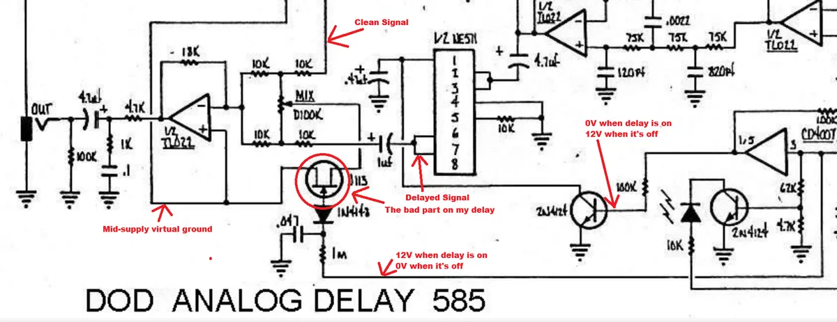
When the pedal is on, a logic high goes to the gate of the J113 JFET circled above, turning it on, and passing the circuit's virtual ground (around 9V on this pedal) to the middle of the mix control. The mix control sweeps that voltage (which, again, is acting like "ground" here) between the clean signal and the delayed signal. At extremes, it's shorting either the clean or delayed signal to "ground," i.e. in this case, the same voltage that's going to the non-inverting (+ labelled) input to the output op-amp TL072.
Over on the right you see the inverted copy of the toggle voltage (low when the pedal is on) going to the base of a BJT transistor. When the base voltage is held low (right around 0V), that BJT looks like an open circuit to pin 1 of the NE571, so that pin happily sits at whatever voltage the compandor wants it to be and signal passes.
When the pedal is off, a logic low to the JFET closes off the path through the J113 and shorts pin 1 of the NE571 to ground, removing the ability to sweep connection to virtual ground via the mix knob while also shutting off the audio path for the delayed signal through the NE571.
And so, after verifying that the actual toggle behavior was working just behind, I concluded that my problem is a fried J113.
JFETs are known for having exceptionally low leakage current on their gates (picoamps, usually), but when I apply 12V from the toggle circuit to the 1M resistor near the bottom of the frame above, I get about 1 volt of drop, meaning I see 11 volts on the other side of the resistor. Ohm's law tells me that means about 1 micro amp of current through the resistor and ultimately into the gate of the JFET, which is two whole orders of magnitude more than the picoamps I expected. The JFET's borked. I've got a replacement on order. Maybe I'm wrong about all this and I'll update if that turns out to be the case!
One last fun note: a lot of modern pedals use an inverter IC to create bi-polar voltage rails to power their high headroom analog circuits. They take in standard pedal 9V and invert it to create +/-9V for 18V of headroom. Not this pedal. It brings in 20V and creates a virtual ground that, in practice, ends up around 9V. It achieves the same thing as a bipolar supply, and is probably ultimately quieter because you're not putting an extra switching regulator on your board, but it sometimes makes reading schematics less intuitive, at least for me.
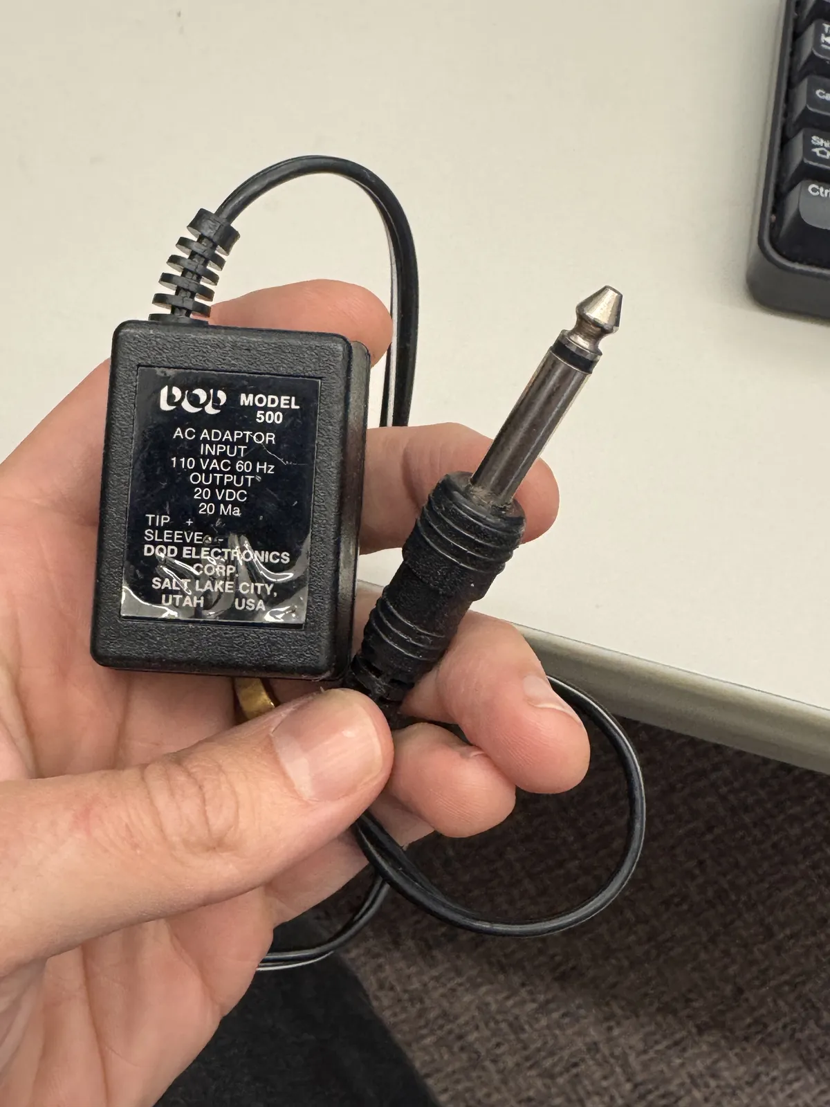
Anyway, the fun part is that this pedal, for some reason gets power not from the standard issue barrel jack but from a 1/4" audio-style jack. There's 20V on the tip and ground on the sleeve. That's totally fine from a current supply perspective, but boy howdy does it create a spark every time you plug it in and accidentally touch the tip to any metal on the pedal. As far as I can tell, there's plenty of protection everywhere to prevent the spark from damaging much, but weird design.